
Graphene synthesis
The optimization of graphene production is a fundamental preliminary step for graphene-based technology. At DSFTM, several synthesis methods are investigated, ranging from chemical vapor deposition (CVD), to SiC graphitization, to organic synthesis and more. In particular, CVD, widely used for large-scale production of macroscopic layers, is studied experimentally and by means of ab-initio calculations, both on substrates of industrial interest (Cu, Ni), at ambient pressure and at low pressure, and on more precious substrates (Pt, Pd, Ir, Ru), for the comprehension of fundamental mechanisms involved in the growth process. To be integrated in real devices, CVD-grown graphene typically requires to be transferred on a different substrate. By graphitization of SiC, it is instead possible to grow graphene layers directly on top of an insulating substrate. This facilitates the formation of hetero-structures and the design of devices. At DSFTM, synthesis mechanisms, atomic structure and transport properties of epitaxial graphene layers on SiC are investigated, as well as the effects on such layers of doping introduced during growth and of intercalation. Besides CVD and SiC graphitization, alternative graphene synthesis methods are studied, to introduce intrinsic flexibility in terms of coupling to different substrates, intrinsic doping and possible functionalization. At DSFTM, alternative methods include organic synthesis, ink-jet printing and photoreduction of graphene oxide. The formation of heterostructures in which graphene is coupled to other 2D materials, and the functionalization by means of deposition of metallic clusters, organic molecules, and hetero-atoms are studied with both experimental and theoretical approach.
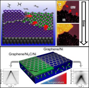 The investigation of CVD graphene growth on Ni(111) under in-operando conditions via complementary in situ STM and XPS allows clarifying the atomistic mechanisms involved in graphene production. When exposing to ethylene a Ni(111) substrate kept at temperatures between 400°C and 600°C, the main growth routes are defined by the catalyst temperature and initial carbon contamination, with different concurring atomic scale mechanisms (top). Upon cooling, additional carbon structures form exclusively underneath rotated graphene domains and decouple the 2D carbon network from the substrate, almost completely restoring its semimetal nature, as demonstrated by combining structure-sensitive LEEM and LEED, with XPEEM and micro-ARPES. The formation and dissolution of the decoupling layer can be easily and reproducibly controlled by the temperature, suggesting a new strategy for the design of controllable graphene/metal interfaces in functional devices (bottom). Source: C. Africh et al., Sci. Rep. 6, 19734 (2016).
Fundamental Properties
At DSFTM there is an intense research activity on the fundamental electronic, optical, magnetic, mechanical, and thermal properties of graphene, both as isolated and as supported material. The electronic interaction of graphene with different substrates, contacts and active layers are investigated, also at the nanoscale, in order to identify effective architectures for novel devices. Leading edge experimental techniques and advanced theoretical methods are used to study electronic structure, bandgap behavior and mobility, electron-phonon interactions, transport in the presence of doping and in nanostructured graphene and mechanisms limiting the transport. For epitaxial graphene, the research work concerns the interaction with the substrate in terms of morphological and transport properties, the latter also in the presence of defects, the relation between electronic properties and structural effects, and the control of Dirac states through doping and chemical effects. Optical and magnetic properties of graphene are also investigated. Main research topics are optical conductivity, nonlinear optics and optomechanics, plasmonics in single layer graphene, graphene/insulator systems as plasmonic platforms for IR and terahertz detectors, interactions between graphene and magnetic substrates. Research activity, mainly theoretical, is focused on the thermodynamic and elastic properties of graphene. The excellent intrinsic thermal properties of graphene are relevant for the identification of architectures capable of limiting thermal anisotropy and optimizing thermal contacts. Moreover the study of nanoscale friction is a means to evaluate the coupling between graphene and supports. In this context the main research topics in DSFTM are thermal conductivity and dissipation in single layer graphene, the effect of strain on the bandgap, and the friction in graphene and related materials.
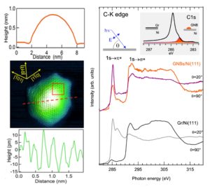 The possibility to intercalate noble gas atoms below epitaxial graphene (Gr) monolayers coupled with the instability at high temperature of Gr on the surface of certain metals has been exploited to produce Ar-filled Gr nanosized blisters (GNBs) evenly distributed on the bare Ni(111) surface. The GNBs contain Ar aggregates compressed at high pressure arranged below the Gr skin that is sealed only at the periphery through stable C−Ni bonds. High resolution STM images show that Gr is not uniformly strained along the bubble profile due to the inhomogeneous expansion of the flexible lattice. The C-K edge NEXAFS spectrum showing the sharp p* feature typical of nearly free standing Gr demonstrates that for the large majority of the C atoms the interaction with the Ni substrate is switched off. The GNBs supported on Ni represents a clean, stable, easy to handle benchmark for fundamental studies and application-oriented investigations in many fields including thermomechanics, nanotribology, optoelectronics, nanomagnetism, and chemistry of graphene. Source: R. Larciprete et al., Nano Lett. 16, 1808-1817 (2016).
Graphene devices
Due to its record opto-electro-mechanical properties, Graphene has been indicated since its discovery as the reference material for application in future ultimately scaled electronic devices and in the portfolio of diversified technologies (from the RF/analog to the biochip) commonly indicated as the “More than Moore” . Research groups at DSFTM are strongly active in exploring the possible applications of graphene, its derivatives (e.g. graphene oxide) and other two dimensional materials in devices technologies. These applicative studies are complemented by experimental and theoretical investigations exploring the fundamental properties of bulk and nanostructured materials (e.g. graphene ribbons or dots) when they interact with electromagnetic field or with different chemical environments. Here we briefly describe the main research interests in this field. Memory and logic functionalities are explored in conventional three terminal prototype structures. Spintronic devices are fabricated, simulated and characterized, where graphene is applied both as active material and a charge and/or spin transporter. Integration of graphene in smart devices fabricated on flexible substrates is explored by research groups with a longstanding experience in the field of the flexible electronics. Technological design and realization of RF devices based on 2D-3D junctions between graphene and large gap semiconductors (SiC, GaN, AlGaN) is under study and the properties of this junction are cleared up relating atomic structure and local measurements of the electron transport. At DSFTM: planar graphene, planar graphene derivatives, hybrid structures, foams and other micro- and nanostructured graphene systems are extensively used to fabricate innovative sensors, where large exposed area, flexible functionalization and easy manipulation, achievable with this 2D material, could be the key ingredients for the successful application in sensing. Graphene based optoelectronic and photonic devices are realized also in view of application in the quantum technologies. In the latter application the role and the control of plasmonic excitations in graphene for the device operation is one of the intriguing aspects under study.
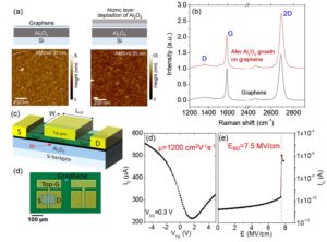 Graphene field effect transistor (GFET) with high-k gate dielectric (Al2O3) grown by optimized atomic layer deposition (ALD) process: (a) Schematic illustration of the Al2O3/graphene stack and surface morphologies of pristine graphene and after ALD deposition of Al2O3. (b) Raman spectra indicating that graphene quality is preserved after the ALD growth. Schematic representation (c) and optical microscopy (d) of GFETs. Transfer characteristic (e) and gate leakage current (f) of the GFET, showing a field effect mobility of 1200 cm2V-1s-1 and a gate dielectric breakdown field of 7.5 MV/cm. Source: G. Fisichella et al., ACS Applied Materials & Interfaces 9, 7761-7771 (2017).
Renewable energies
At CNR DSFTM, graphene is explored for its use in energy production from renewable sources (photovoltaics) and for energy storage. In solar cells, graphene has been integrated both as electrodes and as active material. Due to its high transparency and electrical conductivity, graphene is a promising material for transparent electrodes. An added value is its flexibility and mechanical strength which allows its use even in flexible solar cells. Graphene is also studied as an active material for light harvesting. Working photodetectors based on graphene’s particular plasmonic properties have already been realized, and this know-how is now being transferred to solar cells. Another aspect of green economy is energy storage, be it as chemical or electrical energy. An energy vector par excellence is hydrogen, its only combustion byproduct being water. DSFTM is active in this field, investigating the fundamental interactions between hydrogen and graphene. Furthermore, graphene is considered for hydrogen production, either as carrier of catalytic nanoparticles or via direct photocatalytic water-splitting reaction. Also hydrogen storage in graphene is investigated, both in form of chemisorption and physisorption. Finally, graphene-based bio-fuel cells are developed which allow converting the chemical energy stored in hydrogen into electricity. An alternative approach is to store electrical energy directly via batteries and supercapacitors. Here, Li-functionalized 3D graphene frameworks are investigated as electrode material.
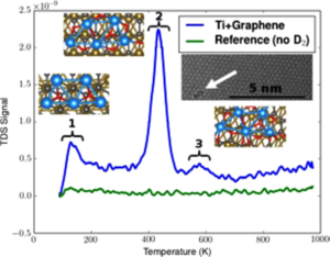 Hydrogen adsorption on graphene-supported metal clusters has brought much controversy due to the complex nature of the bonding between hydrogen and metal clusters. The bond types of hydrogen and graphene-supported Ti clusters are experimentally and theoretically investigated. Transmission electron microscopy shows that Ti clusters of nanometer size are formed on graphene. Thermal desorption spectroscopy captures three hydrogen desorption peaks from hydrogenated graphene-supported Ti clusters. First-principles calculations also found three types of interaction: two types of bonds with different partial ionic character, and physisorption. The physical origin for this rests on the charge state of the Ti clusters: when Ti clusters are neutral, H2 is dissociated, and H forms bonds with the Ti cluster. On the contrary, H2 is adsorbed in molecular form on positively charged Ti clusters, resulting in physisorption. Thus, this work clarifies the bonding mechanisms of hydrogen on graphene-supported Ti clusters. Source: K. Takahashi et al., J. Phys. Chem. C 120, 12974−12979 (2016).