
Micro– nanoelectronics are one of the European Programme Horizon 2020 key enabling technologies (KET). They are not only relevant for many services and products, but also underlie innovation and competitiveness of most sector of the National Research Plan. The DSFTM activities in this field are focused on a series of areas strongly linked to companies in the National territory (STMicroelectronics, LFoundry) and at European research centres (CEA–LETI, IMEC) and aim at the development of new materials, processes, devices and technologies in the following main sectors:
- Devices on nanometer scale with new generation logic and/or memory functionality based on emerging concepts.
- Non–electronic systems for the development of multifunctional platforms (More than Moore) and innovative computational architecture.
- Enabling technologies for new generation high–frequency, power devices based on advanced materials (SiC, GaN, GaAs, graphene, etc.).
- Devices for energy conversion working through photo–thermoionic, thermoionic and thermoelectrical processes based on non–conventional materials and on nanostructures;
- Devices and electronic circuits on flexible substrates based both on organic transistors (OTFTs), realized by means of fully printed technology, and on polycrystalline silicon TFT.
- Realization of autonomous multisensorial systems for chemical and physical parameters; multifunctional and multisensorial systems for: ambient–assisted living; health safety and security and healthcare prevention; agri–food chain monitoring.
- Advanced MEMS/MOEMS technologies for deformation resonating sensors, energetic micro–harvesting, pressure, inertial, acoustic and including the integration of innovative materials and 2D (graphene, MoS2) for piezoelectrical, thermoelectrical and chemical transduction.
- Multifunctional systems for biomedical applications: biosensors, drugs micro–dispensers medical diagnostic systems (breath analysis, PET analysis, myocardial infarction), MOEMS on optical fibres for medical diagnosis.
Spotlights on research activity
Photovoltaic Anodes for Enhanced Thermionic Energy Conversion
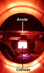
Thermionic energy converters are heat engines based on the direct emission of electrons from a hot cathode toward a colder anode. Because the thermionic emission is unavoidably accompanied by photonic emission, radiative energy transfer is a significant source of losses in these devices. We have provided the experimental demonstration of a hybrid thermionic–photovoltaic device that is able to produce electricity not only from the electrons but also from the photons that are emitted by the cathode. Thermionic electrons are injected in the valence band of a gallium arsenide semiconducting anode, then pumped to the conduction band by the photovoltaic effect, and finally extracted from the conduction band to produce useful energy before they are reinjected in the cathode. We have shown that such a hybrid device produces a voltage boost of about 1 V with
respect to a reference thermionic device made of the same materials and operating under the same conditions. This proof of concept paves the way to the development of efficient thermionic and photovoltaic devices for the direct conversion of heat into electricity.
Contact person: Daniele Trucchi, ISM Roma Tor Vergata
Large–area patterning of substrate–conformal MoS2 nano–trenches
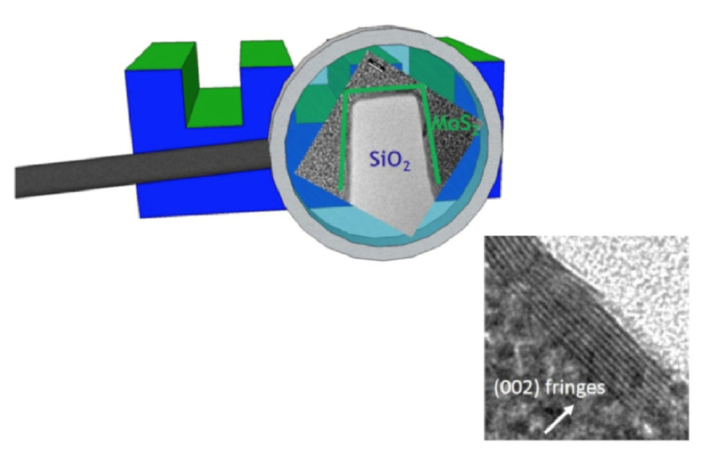
Within the class of two–dimensional materials, transition metal dichalcogenides (TMDs), are extremely appealing for a variety of technological applications. Moreover, the manipulation of the layered morphology at the nanoscale is a knob for further tailoring their physical and chemical properties towards target applications. The combination of atomic layer deposition (ALD) and chemical vapour deposition (CVD) has been presented as a general approach for the fabrication of TMD layers arranged in arbitrary geometry at the nanoscale. Indeed, following such all–chemical based approach, high–resolution electron microscopy shows the conformal growth of MoS2 to nano– trench pattern obtained in SiO2 substrates on large area. Growth is uniform not only in the flat region of the pattern but also at the hinges and throughout vertical faces, without rupture, all along the rectangular shape profile of the trenches. Furthermore, MoS2 bending dramatically affects the electron–phonon coupling as demonstrated by resonant Raman scattering. The proposed approach opens the door to the on-demand manipulation of the TMDs properties by large-scale substrate pattern design.
Contact person: Christian Martella, IMM Agrate Brianza
Ohmic contacts to gallium nitride materials
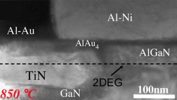
A comprehensive study of the mechanisms of Ohmic contact formation on GaN–based materials has been addressed. The optimal metallization schemes and processing conditions to obtain low resistance Ohmic contacts have been investigated, discussing the role of the single metals composing the stack and the modification induced by the thermal annealing, either on the metal layers or at the interface with GaN. Physical insights on the mechanism of Ohmic contact formation have been gained by correlating the temperature dependence of the electrical parameters with a morphological/structural analysis of the interface. In the case of the AlGaN/GaN systems, the influence of the heterostructure parameters on the Ohmic contacts has been taken into account adapting the classical thermionic field emission model to the presence of the two–dimensional electron gas. Finally, the “Au-free” metallization to AlGaN/GaN heterostructures has been deeply investigated, being this latter a relevant topic for the integration of GaN technology on large scale silicon devices fabrication.
Contact person: Giuseppe Greco, IMM Catania
Control of doping level in semiconductors via self–limited grafting of phosphorus end terminated polymers
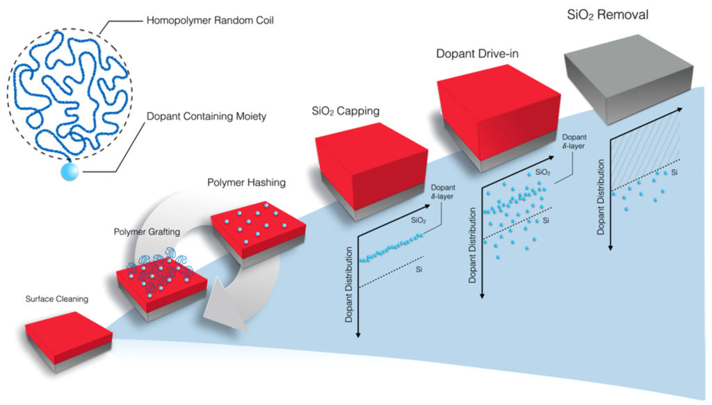
An effective bottom–up technology for precisely controlling the amount of dopant atoms tethered on silicon substrates has been presented. Polystyrene and poly (methyl methacrylate) polymers with narrow molecular weight distribution and end–terminated with a P–containing moiety were synthesized with different molar mass. The polymers were spin coated and subsequently end-grafted onto nondeglazed silicon substrates. P atoms were bonded to the surface during the grafting reaction, and their surface density was set by the polymer molar mass, according to the self-limiting nature of the “grafting to” reaction. Polymeric material was removed by O2 plasma hashing without affecting the tethered P–containing moieties on the surface. Repeated cycles of polymer grafting followed by plasma hashing led to a cumulative increase, at constant steps, in the dose of P atoms grafted to the silicon surface. P injection in the silicon substrate was promoted and precisely controlled by high–temperature thermal treatments. Sheet resistance measurements demonstrated effective doping of silicon substrate.
Contact person: Michele Perego, IMM Agrate Brianza
Kinetic Inductance Detector (KID) Arrays for the OLIMPO programme
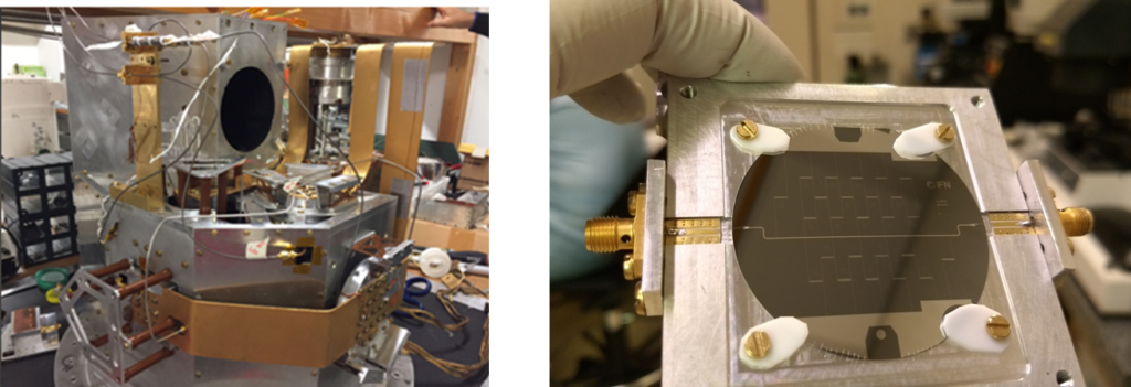
Kinetic Inductance Detectors (KIDs) are a novel type of superconducting photon detectors firstly developed in 2003 and currently employed in several research fields. In particular, they got a rapid employment in astrophysics as high-sensitivity detectors for frequencies ranging from the far-infrared to X-rays. In the framework of the OLIMPO mission, an Italian programme in collaboration with Sapienza University in Rome, we developed four KID arrays simultaneously investigating four different bands of the microwave spectrum (centred at 150 GHz, 200 GHz, 350 GHz, and 480 GHz). They will be mounted on the OLIMPO telescope with the aim of measuring the anisotropy of cosmic microwave background radiation and cluster of galaxies and early galaxies with unparalleled precision. The OLIMPO’s KID arrays have been realized by electron beam lithography, thin film deposition and lift-off processes. They consist of 23 to 43 KIDs patterned in a 25-nm thick aluminium film on high resistivity Si wafers connected capacitively to a same coplanar feedline for their simultaneous reading. OLIMPO will be the first telescope equipped with KIDs and mounted on a long-term stratospheric balloon to fly. The mission will be launched by ASI in June 2018.
Contact person: Giorgio Pettinari, IFN - CNR Roma
Detection of food and skin pathogen microbiota by means of an electronic nose based on metal oxide chemiresistors
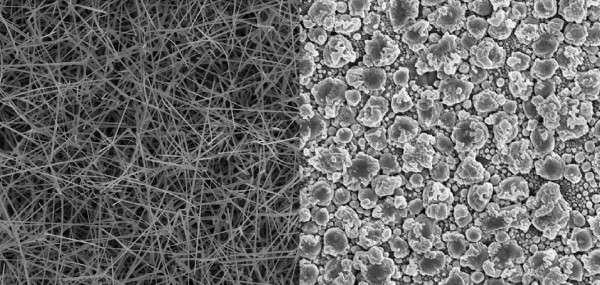
We have analyzed the potentiality of a mixed array merging the nanowire and thin film metal oxide technologies to develop an electronic nose as a tool to monitor the human skin and food pathogen microbiota. Nanowire and thin film sensors have been fabricated, characterized and then integrated together to develop a hybrid device that can enhance the sensing performance. Different blends of microorganisms grown in artificial sweat have been tested. Classical techniques, like gas chromatography–mass spectrometry (GC–MS) with solid phase micro extraction (SPME) have been employed in parallel, in order to have a multidisciplinary approach and a consistent data set. The obtained results demonstrate the potentiality of the proposed electronic nose to discriminate between the different blends of microorganisms and to follow up microbiota growth inside the blends.
Contact person: Estefanìa Nùñez Carmona, INO Brescia
Interface electrical properties of Al2O3 thin films on graphene obtained by atomic layer deposition with an in situ seedlike layer
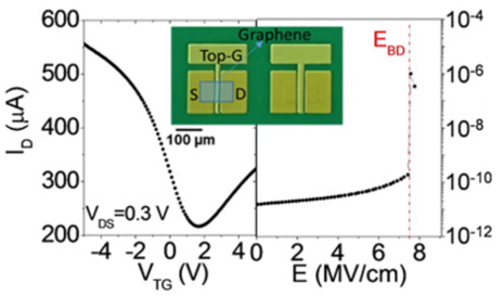 High–quality thin insulating films on graphene (Gr) are essential for field-effect transistors (FETs) and other electronics applications of this material. We have reported a detailed morphological, structural, and electrical investigation of Al2O3 thin films grown by a two–steps ALD process on a large area Gr membrane residing on an Al2O3–Si substrate. This process consists of the H2O–activated deposition of a Al2O3 seed layer a few nanometers in thickness, performed in situ at 100 °C, followed by ALD thermal growth of Al2O3 at 250 °C. Nanoscale–resolution mapping of the current through the dielectric by conductive atomic force microscopy (CAFM) demonstrated an excellent laterally uniformity of the film. Analysis of the transfer characteristics of Gr field–effect transistors (GFETs) allowed us to evaluate the relative dielectric permittivity (ε = 7.45) and the breakdown electric field (EBD = 7.4 MV/cm) of the Al2O3 film as well as the transconductance and the holes field-effect mobility (about 1200 cm2 V–1 s–1).
Contact person: Gabriele Fisichella, IMM Catania
Ambipolar MoS2 transistors by nanoscale tailoring of Schottky barrier using oxygen plasma functionalization
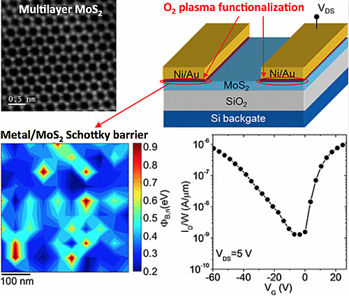 Hole transport in MoS2 field–effect transistors (FETs) is typically hampered by the high Schottky barrier height (SBH) for holes at source/drain contacts, due to the Fermi level pinning close to the conduction band. We have shown that the SBH of multilayer MoS2 surface can be tailored at nanoscale using soft O2 plasma treatments. Nanoscale current–voltage mapping by Conductive Atomic Force Microscopy showed that the SBH maps can be conveniently tuned starting from a narrow SBH distribution (from 0.2 to 0.3 eV) in the case of pristine MoS2 to a broader distribution (from 0.2 to 0.8 eV) after 600 s O2 plasma treatment, which allows both electron and hole injection. Back-gated multilayer MoS2 FETs, fabricated by self–aligned deposition of source/drain contacts in the O2 plasma functionalized areas, exhibit ambipolar current transport with on/off current ratio Ion/Ioff ≈ 103 and field–effect mobilities of 11.5 and 7.2 cm2 V–1s–1 for electrons and holes, respectively.
Contact person: Filippo Giannazzo, IMM Catania
Organic gelators as growth control agents for stable and reproducible hybrid perovskite–based solar cells
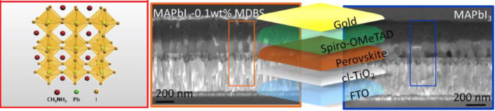
We have used the concept based on low molecular–weight organic gelators to hybrid halide perovskite–based materials. Our measurements reveal that organic gelators beneficially influence the nucleation and growth of the perovskite precursor phase. This can be exploited for the performance that not only is enhanced by about 25% compared to solar cells where the active layer was produced without the use of a gelator but that also feature a higher stability to moisture and a reduced hysteresis. The proposed approach provides a general method to render the film–formation of hybrid perovskites more reliable and robust.
Contact person: Silvia Colella, NANOTEC-CNR Lecce
Resistive switching in high–density nanodevices fabricated by block copolymer self–assembly
By exploiting a bottom-up fabrication approach based on block copolymer self-assembling, we obtained the parallel production of bilayer Pt/Ti top electrodes arranged in periodic arrays over the HFO2/TiN surface, building memory devices with a diameter of 28 nm and a density of 5´1010 devices/cm2. For an electrical characterization, the sharp conducting tip of an atomic force microscope was adopted for a selective addressing of the nanodevices. The presence of devices showing high conductance in the initial state was directly connected with scattered leakage current paths in the bare oxide film, while with bipolar voltage operations we obtained reversible set/reset transitions irrespective of the conductance variability in the initial state.
Contact person: Michele Perego, IMM–CNR Agrate Brianza
Micromotors with asymmetric shape that efficiently convert light into work by thermocapillary effects
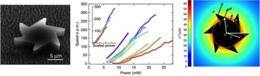
The direct conversion of light into work allows the driving of micron-sized motors in a contactless, controllable and continuous way. We have shown that microfabricated gears, sitting on a liquid–air interface, can efficiently convert absorbed light into rotational motion through a thermocapillary effect. We have demonstrated rotation rates up to 300 r.p.m. under wide–field illumination with incoherent light. Our analysis shows that thermocapillary propulsion is one of the strongest mechanisms for light actuation at the micron– and nanoscale.
Contact person: Claudio Maggi, NANOTEC–CNR Roma
Silicene field-effect transistors operating at room temperature
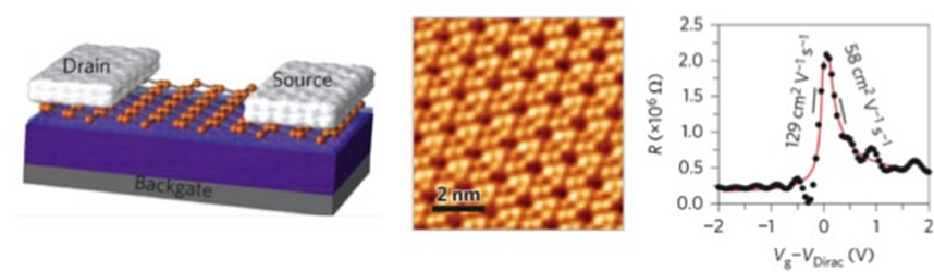
We have reported a silicene field–effect transistor, corroborating theoretical expectations regarding its ambipolar Dirac charge transport, with a measured room–temperature mobility of about 100 cm2 V–1 s–1 attributed to acoustic phonon–limited transport and grain boundary scattering. These results are enabled by a growth–transfer–fabrication process that we have devised silicene encapsulated delamination with native electrodes. This approach addresses a major challenge for material preservation of silicene during transfer and device fabrication and is applicable to other air–sensitive two–dimensional materials such as germanene and phosphorene. Silicene’s allotropic affinity with bulk silicon and its low-temperature synthesis compared with graphene or alternative two–dimensional semiconductors suggest a more direct integration with ubiquitous semiconductor technology.
Contact person: Alessandro Molle, IMM–CNR Agrate Brianza