
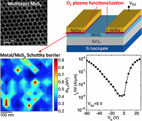
 Hole transport in MoS2 field–effect transistors (FETs) is typically hampered by the high Schottky barrier height (SBH) for holes at source/drain contacts, due to the Fermi level pinning close to the conduction band. We have shown that the SBH of multilayer MoS2 surface can be tailored at nanoscale using soft O2 plasma treatments. Nanoscale current–voltage mapping by Conductive Atomic Force Microscopy showed that the SBH maps can be conveniently tuned starting from a narrow SBH distribution (from 0.2 to 0.3 eV) in the case of pristine MoS2 to a broader distribution (from 0.2 to 0.8 eV) after 600 s O2 plasma treatment, which allows both electron and hole injection. Back-gated multilayer MoS2 FETs, fabricated by self–aligned deposition of source/drain contacts in the O2 plasma functionalized areas, exhibit ambipolar current transport with on/off current ratio Ion/Ioff ≈ 103 and field–effect mobilities of 11.5 and 7.2 cm2 V–1s–1 for electrons and holes, respectively.
Contact person: Filippo Giannazzo, IMM Catania