
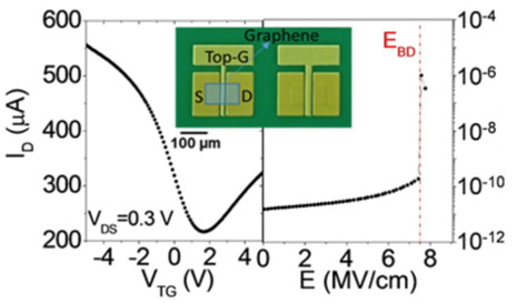
 High–quality thin insulating films on graphene (Gr) are essential for field-effect transistors (FETs) and other electronics applications of this material. We have reported a detailed morphological, structural, and electrical investigation of Al2O3 thin films grown by a two–steps ALD process on a large area Gr membrane residing on an Al2O3–Si substrate. This process consists of the H2O–activated deposition of a Al2O3 seed layer a few nanometers in thickness, performed in situ at 100 °C, followed by ALD thermal growth of Al2O3 at 250 °C. Nanoscale–resolution mapping of the current through the dielectric by conductive atomic force microscopy (CAFM) demonstrated an excellent laterally uniformity of the film. Analysis of the transfer characteristics of Gr field–effect transistors (GFETs) allowed us to evaluate the relative dielectric permittivity (ε = 7.45) and the breakdown electric field (EBD = 7.4 MV/cm) of the Al2O3 film as well as the transconductance and the holes field-effect mobility (about 1200 cm2 V–1 s–1).
Contact person: Gabriele Fisichella, IMM Catania