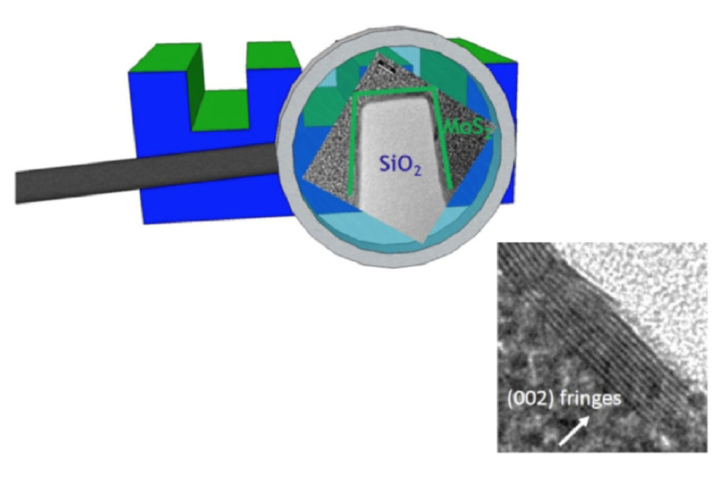
Within the class of two–dimensional materials, transition metal dichalcogenides (TMDs), are extremely appealing for a variety of technological applications. Moreover, the manipulation of the layered morphology at the nanoscale is a knob for further tailoring their physical and chemical properties towards target applications. The combination of atomic layer deposition (ALD) and chemical vapour deposition (CVD) has been presented as a general approach for the fabrication of TMD layers arranged in arbitrary geometry at the nanoscale. Indeed, following such all–chemical based approach, high–resolution electron microscopy shows the conformal growth of MoS2 to nano– trench pattern obtained in SiO2 substrates on large area. Growth is uniform not only in the flat region of the pattern but also at the hinges and throughout vertical faces, without rupture, all along the rectangular shape profile of the trenches. Furthermore, MoS2 bending dramatically affects the electron–phonon coupling as demonstrated by resonant Raman scattering. The proposed approach opens the door to the on-demand manipulation of the TMDs properties by large-scale substrate pattern design.
Contact person: Christian Martella, IMM Agrate Brianza
