Planar nanoactuators based on VO2 phase transition

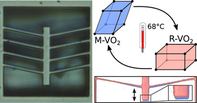
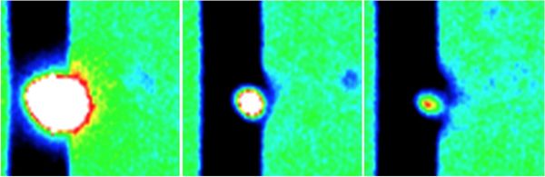
Actuation at micro– and nanoscale often requires large displacements and applied forces. The high work energy density that lies inside many phase transitions is an appealing feature for developing new actuating schemes, especially if the transition is reversible and scalable into small actuating domains. We have shown the fabrication of a planar nanomechanical actuator having chevron–type geometry and based on the phase transition of VO2. This device is thermally activated through heating just above room temperature to trigger the VO2 crystalline symmetry change associated with the metal–insulator transition. The large lattice expansion of VO2 phase transition, compared to standard materials, is further amplified by the chevron–type geometry. DC and AC operation of the device are discussed.

Contact person: Nicola Manca, SPIN Genova

Pb clustering and PbI2 nanofragmentation during methylammonium lead iodide perovskite degradation

Studying defect formation and evolution in MethylAmmonium lead Iodide (MAPbI3) perovskite layers has a bottleneck in the softness of the matter and in its consequent sensitivity to external solicitations. We have reported that, in a polycrystalline MAPbI3 layer, Pb–related defects aggregate into nanoclusters preferentially at the triple grain boundaries as unveiled by Transmission Electron Microscopy (TEM) analyses at low total electron dose. Pb–clusters are killer against MAPbI3 integrity since they progressively feed up the hosting matrix. This progression is limited by the concomitant but slower transformation of the MAPbI3 core to fragmented and interconnected nano-grains of 6H–PbI2 that are structurally linked to the mother grain as in strain-relaxed heteroepitaxial coupling. The phenomenon occurs more frequently under TEM degradation whilst air degradation is more prone to leave uncorrelated [001]-oriented 2H–PbI2 grains as statistically found by X–Ray Diffraction. This path is kinetically costlier but thermodynamically favoured and is easily activated by catalytic species.

Contact person: Alessandra Alberti, IMM Catania

Nitrogen Soaking Promotes Lattice Recovery in Polycrystalline Hybrid Perovskites

A research team from two Institutes, IMM and NANOTEC, has found a very important innovative result in the field of photovoltaics applications by using hybrid Perovskites and Nitrogen.

Hybrid Perovskites are innovative materials that are sensitive to solar light with high conversion photon-electron performances.  Nitrogen is soaked into polycrystalline MAPbI3 via a post deposition mild thermal treatment under slightly overpressure conditions to promote its diffusion across the whole layer. A significant reduction of radiative recombination and a concurrent increase of light absorption, with a maximum benefit at 80 °C, are observed.

The achieved improvements are linked to a nitrogen‐assisted recovery of intrinsic lattice disorder at the grain shells along with a simultaneous stabilization of under-coordinated Pb2+ and MA+ cations through weak electrostatic interactions. Defect mitigation under N2 is reinforced in comparison to the benchmark behaviour under argon.

Such simple and low‐cost strategy can complement other stabilizing solutions for perovskite solar cells or light‐emitting diode engineering.

Contact persons: Alessandra Alberti - IMM Catania
Silvia Colella - NANOTEC Lecce

Mechanisms and processes of pulsed laser ablation in liquids during nanoparticle production

In the last decade Pulsed Laser Ablation in Liquids (PLAL) has been widely investigated from the fundamental point of view, and various theories have been proposed. We have reconsidered previous works focused on specific processes and stages of the PLAL, in order to outline a modern and comprehensive point of view of the overall physical aspects of PLAL. With this aim, several simultaneous diagnostic methods have been applied during the production of metallic nanoparticles (NPs), i.e. optical emission spectroscopy and fast imaging for the investigation of the laser-induced plasma, shadowgraph for the study of the cavitation bubble, and Double Pulse Laser Ablation in Liquid (DP–LAL) and laser scattering for the investigation of NPs location and mechanisms of release in solution. The connection between the various stages of the DP–LAL allows understanding the main characteristics of the produced NPs and the typical timescales of the basic mechanisms involved in PLAL.

Contact person: Marcella Dell’Aglio, NANOTEC Bari

Spectral imaging and archival data in analysing Madonna of the rabbit paintings by Manet and Titian

A concise insight into the outputs provided by the latest prototype of visible–near infrared (Vis-NIR) multispectral scanner was presented. The analytical data acquired on an oil painting Madonna of the Rabbit by E. Manet were described. In this work, the Vis-NIR was complemented with X–ray fluorescence (XRF) mapping for the chemical and spatial characterization of several pigments. The spatially registered Vis–NIR data facilitated their processing by spectral correlation mapping (SCM) and artificial neural network (ANN) algorithm, respectively, for pigment mapping and improved visibility of pentimenti and of underdrawing style. The data provided several key elements for the comparison with a homonymous original work by Titian studied within the ARCHive LABoratory (ARCHLAB) transnational access project.

Contact person: Jana Striova, INO Florence

Carbon nanotubes as excitonic insulators

Fifty years ago Walter Kohn speculated that a zero-gap semiconductor might be unstable against the spontaneous generation of excitons–electron–hole pairs bound together by Coulomb attraction. The reconstructed ground state would then open a gap breaking the symmetry of the underlying lattice, a genuine consequence of electronic correlations. We have shown that this excitonic insulator is realized in zero–gap carbon nanotubes by performing first–principles calculations through many–body perturbation theory as well as quantum Monte Carlo. The excitonic order modulates the charge between the two carbon sublattices opening an experimentally observable gap, which scales as the inverse of the tube radius and weakly depends on the axial magnetic field. Our findings call into question the Luttinger liquid paradigm for nanotubes and provide tests to experimentally discriminate between excitonic and Mott insulators.

Contact person: Daniele Varsano, NANO Modena

Rational design of molecular hole–transporting materials for perovskite solar cells: direct versus inverted device configurations

Due to a still limited understanding of the reasons making 2,2/,7,7/–tetrakis(N,N–di–p–methoxyphenylamine)–9,9/–spirobifluorene (Spiro–OMeTAD) the state–of–the–art hole–transporting material (HTM) for emerging photovoltaic applications, the molecular tailoring of organic components for perovskite solar cells (PSCs) lacks in solid design criteria. Charge delocalization in radical cationic states can undoubtedly be considered as one of the essential prerequisites for an HTM, but this aspect has been investigated to a relatively minor extent. In marked contrast with the 3–D structure of Spiro–OMeTAD, truxene–based HTMs Trux1 and Trux2 have been employed for the first time in PSCs fabricated with a direct (nip) or inverted (pin) architecture, exhibiting a peculiar behavior with respect to the referential HTM. Notwithstanding the efficient hole extraction from the perovskite layer exhibited by Trux1 and Trux2 in direct configuration devices, their photovoltaic performances were detrimentally affected by their poor hole transport. Conversely, an outstanding improvement of the photovoltaic performances in dopant–free inverted configuration devices compared to Spiro–OMeTAD was recorded, ascribable to the use of thinner HTM layers. The rationalization of the photovoltaic performances exhibited by different configuration devices discussed in this paper can provide new and unexpected prospects for engineering the interface between the active layer of perovskite–based solar cells and the hole transporters.

Contact person: Luisa De Marco, NANOTEC Lecce

Electronic states of silicene allotropes on Ag(111)

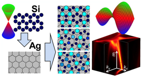
We have compared the electronic structure of (4×4), (√13×√13) R 13.9° and (2√3×2√3) R 30° silicene monolayers on Ag(111) by means of angle–resolved photoemission spectroscopy and first–principles calculations. We have found that all phases display similar Ag–derived interface states and s bands weakly perturbed by the substrate interaction. Intense spectral features, including those previously attributed to s band emission from the (2√3×2√3) R 30° structure, are found to originate from umklapp replicas of the Ag interface state and Ag sp–bulk bands. All the examined silicene allotropes do not display the characteristic Dirac cones of free–standing silicene, proving that the p bands are strongly modified by the interaction with the substrate bands independently of the structural detail of the allotrope.

Contact person: Polina Sheverdyaeva, ISM Trieste

Tunable Esaki effect in catalyst–free InAs/GaSb core–shell nanowires

We have demonstrated tunable bistability and a strong negative differential resistance in InAs/GaSb core–shell nanowire devices embedding a radial broken–gap heterojunction. Nanostructures have been grown using a catalyst-free synthesis on a Si substrate. Current–voltage characteristics display a top peak–to–valley ratio of 4.8 at 4.2 K and 2.2 at room temperature. The Esaki effect can be modulated – or even completely quenched – by field effect, by controlling the band bending profile along the azimuthal angle of the radial heterostructure. Hysteretic behavior is also observed in the presence of a suitable resistive load. Our results indicate that high–quality broken–gap devices can be obtained using Au–free growth.

Contact person: Mirko Rocci, NANO Pisa

Anisotropic MoS2 nanosheets grown on self–organized nanopatterned substrates

We have presented a novel approach to introduce a one–directional anisotropy in MoS2 nanosheets via chemical vapor deposition (CVD) onto rippled patterns prepared on ion–sputtered SiO2/Si substrates. The optoelectronic properties of MoS2 are dramatically affected by the rippled MoS2 morphology both at the macro– and the nanoscale. In particular, strongly anisotropic phonon modes are observed depending on the polarization orientation with respect to the ripple axis. Moreover, the rippled morphology induces localization of strain and charge doping at the nanoscale, thus causing substantial redshifts of the phonon mode frequencies and a topography–dependent modulation of the MoS2 work–function, respectively. This study paves the way to a controllable tuning of the anisotropy via substrate pattern engineering in CVD–grown 2D nanosheets.

Contact person: Christian Martella, IMM–CNR Agrate Brianza

Atomistic origins of CH3NH3PbI3 degradation to PbI2 in vacuum

We have studied the mechanisms of CH3NH3PbI3 degradation and its transformation to PbI2 by means of X–ray diffraction and the density functional theory. The experimental analysis has shown that the material can degrade in both air and vacuum conditions, with humidity and temperature–annealing strongly accelerating such process. Based on ab–initio calculations, we have argued that even in the absence of humidity, a decomposition of the perovskite structure can take place through the statistical formation of molecular defects with a non–ionic character, whose volatility at surfaces should break the thermodynamic defect equilibrium.

Contact person: Ioannis Deretzis, IMM–CNR Catania

Methylammonium rotational dynamics in lead halide perovskite by classical molecular dynamics: the role of temperature

An interatomic model potential for molecular dynamics was derived from first–principles and used to study the molecular rotations and relaxation times in methylammonium lead halide, considered the prototypical example of a hybrid crystal with a strong reorientational dynamics. Within the limits of a simple ionic scheme, the potential is able to catch the main qualitative features of the material at zero and finite temperature and opens the way to the development of classical potentials for hybrid perovskites. This work has clarified the temperature dependence of the relaxation times and the interpretation of the experimental data in terms of the different mechanisms contributing to the molecule dynamics.

Contact person: Alessandro Mattoni, IOM–CNR Cagliari

Tunable spin polarization and superconductivity in engineered oxide interfaces

We have shown that a fully electric–field–tunable spin–polarized and superconducting quasi–2D electron system (q2DES) can be artificially created by inserting a few unit cells of delta doping EuTiO3 at the interface between LaAlO3 and SrTiO3 oxides. Spin polarization emerges below the ferromagnetic transition temperature of the EuTiO3 layer (TFM = 6–8 K) and is due to the exchange interaction between the magnetic moments of Eu–4f and of Ti–3d electrons. Moreover, in a large region of the phase diagram, superconductivity sets in from a ferromagnetic normal state. The occurrence of magnetic interactions, superconductivity and spin–orbit coupling in the same q2DES makes the LaAlO3/EuTiO3/SrTiO3 system an intriguing platform for the emergence of novel quantum phases in low–dimensional materials.

Contact person: Marco Salluzzo, SPIN–CNR Napoli