Planar nanoactuators based on VO2 phase transition

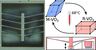
Actuation at micro– and nanoscale often requires large displacements and applied forces. The high work energy density that lies inside many phase transitions is an appealing feature for developing new actuating schemes, especially if the transition is reversible and scalable into small actuating domains. We have shown the fabrication of a planar nanomechanical actuator having chevron–type geometry and based on the phase transition of VO2. This device is thermally activated through heating just above room temperature to trigger the VO2 crystalline symmetry change associated with the metal–insulator transition. The large lattice expansion of VO2 phase transition, compared to standard materials, is further amplified by the chevron–type geometry. DC and AC operation of the device are discussed.

Contact person: Nicola Manca, SPIN Genova

Preferential removal of pesticides from water by molecular imprinting on TiO2 photocatalysts

In order to achieve a selective removal of specific pesticides from water, we synthesized, through the sol–gel technique, molecularly imprinted TiO2 photocatalysts with the only use of the standard reactants of the TiO2 solgel synthesis together with the pesticide molecules, without any addition of further reactants supports or matrices. It is a new, easy, smart and scalable method that avoid the multistep and solvent–consuming procedures, typical of the molecular imprinting. Two widely–used pesticides, i.e. the herbicide 2,4D, and the insecticide imidacloprid, were chosen as template for the molecular imprinting and as contaminants target for the photocatalytic tests. A remarkable enhancement of the photocatalytic activity was verified with the TiO2 imprinted with the corresponding pesticide-target. The selectivity of the photodegradation process was verified thanks to the comparison with the degradation of pesticides not–used as template. Furthermore, the eventual toxic effects of the molecularly imprinted materials were evaluated by biological tests.

Contact person: Roberto Fiorenza, IMM c/o Università di Catania

Photovoltaic Anodes for Enhanced Thermionic Energy Conversion

Thermionic energy converters are heat engines based on the direct emission of electrons from a hot cathode toward a colder anode. Because the thermionic emission is unavoidably accompanied by photonic emission, radiative energy transfer is a significant source of losses in these devices. We have provided the experimental demonstration of a hybrid thermionic–photovoltaic device that is able to produce electricity not only from the electrons but also from the photons that are emitted by the cathode. Thermionic electrons are injected in the valence band of a gallium arsenide semiconducting anode, then pumped to the conduction band by the photovoltaic effect, and finally extracted from the conduction band to produce useful energy before they are reinjected in the cathode. We have shown that such a hybrid device produces a voltage boost of about 1 V with
respect to a reference thermionic device made of the same materials and operating under the same conditions. This proof of concept paves the way to the development of efficient thermionic and photovoltaic devices for the direct conversion of heat into electricity.

Contact person: Daniele Trucchi, ISM Roma Tor Vergata

Measurement of the quantum geometric tensor and of the anomalous Hall drift

Topological physics relies on the structure of the eigenstates of the Hamiltonians. The geometry of the eigenstates is encoded in the quantum geometric tensor – comprising the Berry curvature (crucial for topological matter) and the quantum metric, which defines the distance between the eigenstates. Knowledge of the quantum metric is essential for understanding many phenomena, such as superfluidity in flat bands, orbital magnetic susceptibility, the exciton Lamb shift and the non-adiabatic anomalous Hall effect. However, the quantum geometry of energy bands has not been measured. Here we report the direct measurement of both the Berry curvature and the quantum metric in a two-dimensional continuous medium – a high–finesse planar microcavity – together with the related anomalous Hall drift. The microcavity hosts strongly coupled exciton–photon modes (exciton polaritons) that are subject to photonic spin–orbit coupling from which Dirac cones emerge, and to exciton Zeeman splitting, breaking time-reversal symmetry. The monopolar and half–skyrmion pseudospin textures are measured using polarization- resolved photoluminescence. The associated quantum geometry of the bands is extracted, enabling prediction of the anomalous Hall drift, which we measure independently using high-resolution spatially resolved epifluorescence. Our results unveil the intrinsic chirality of photonic modes, the cornerstone of topological photonics. These results also experimentally validate the semiclassical description of wavepacket motion in geometrically non–trivial bands. The use of exciton polaritons (interacting photons) opens up possibilities for future studies of quantum fluid physics in topological systems.

Contact person: Daniele Sanvitto, NANOTEC Lecce

Room-temperature graphene photodetectors at terahertz frequencies, with High Speed and Low Noise

Uncooled terahertz photodetectors (PDs) showing fast (ps) response and high sensitivity (noise equivalent power (NEP) < nW/Hz1/2) over a broad (0.5–10 THz) frequency range are needed for applications in high-resolution spectroscopy (relative accuracy ∼10–11), metrology, quantum information, security, imaging, optical communications.

However, present terahertz receivers cannot provide the required balance between sensitivity, speed, operation temperature, and frequency range. Here, we demonstrate uncooled terahertz PDs combining the low (∼2000 kB μm–2) electronic specific heat of high mobility (>55 000 cm2 V–1 s–1) hexagonal boron nitride-encapsulated graphene, with asymmetric field enhancement produced by a bow-tie antenna, resonating at 3 THz.  This produces a strong photo-thermoelectric conversion, which simultaneously leads to a combination of high sensitivity (NEP ≤ 160 pW Hz–1/2), fast response time (≤ 3.3 ns), and a 4 orders of magnitude dynamic range, making our devices the fastest, broad-band, low-noise, room-temperature terahertz PD, to date.

Contact: Miriam Serena Vitiello – Istituto Nanoscienze 

Pb clustering and PbI2 nanofragmentation during methylammonium lead iodide perovskite degradation

Studying defect formation and evolution in MethylAmmonium lead Iodide (MAPbI3) perovskite layers has a bottleneck in the softness of the matter and in its consequent sensitivity to external solicitations. We have reported that, in a polycrystalline MAPbI3 layer, Pb–related defects aggregate into nanoclusters preferentially at the triple grain boundaries as unveiled by Transmission Electron Microscopy (TEM) analyses at low total electron dose. Pb–clusters are killer against MAPbI3 integrity since they progressively feed up the hosting matrix. This progression is limited by the concomitant but slower transformation of the MAPbI3 core to fragmented and interconnected nano-grains of 6H–PbI2 that are structurally linked to the mother grain as in strain-relaxed heteroepitaxial coupling. The phenomenon occurs more frequently under TEM degradation whilst air degradation is more prone to leave uncorrelated [001]-oriented 2H–PbI2 grains as statistically found by X–Ray Diffraction. This path is kinetically costlier but thermodynamically favoured and is easily activated by catalytic species.

Contact person: Alessandra Alberti, IMM Catania

Large–area patterning of substrate–conformal MoS2 nano–trenches

Within the class of two–dimensional materials, transition metal dichalcogenides (TMDs), are extremely appealing for a variety of technological applications. Moreover, the manipulation of the layered morphology at the nanoscale is a knob for further tailoring their physical and chemical properties towards target applications. The combination of atomic layer deposition (ALD) and chemical vapour deposition (CVD) has been presented as a general approach for the fabrication of TMD layers arranged in arbitrary geometry at the nanoscale. Indeed, following such all–chemical based approach, high–resolution electron microscopy shows the conformal growth of MoS2 to nano– trench pattern obtained in SiO2 substrates on large area. Growth is uniform not only in the flat region of the pattern but also at the hinges and throughout vertical faces, without rupture, all along the rectangular shape profile of the trenches. Furthermore, MoS2 bending dramatically affects the electron–phonon coupling as demonstrated by resonant Raman scattering. The proposed approach opens the door to the on-demand manipulation of the TMDs properties by large-scale substrate pattern design.

Contact person: Christian Martella, IMM Agrate Brianza

Fully phase-stabilized quantum cascade laser frequency comb

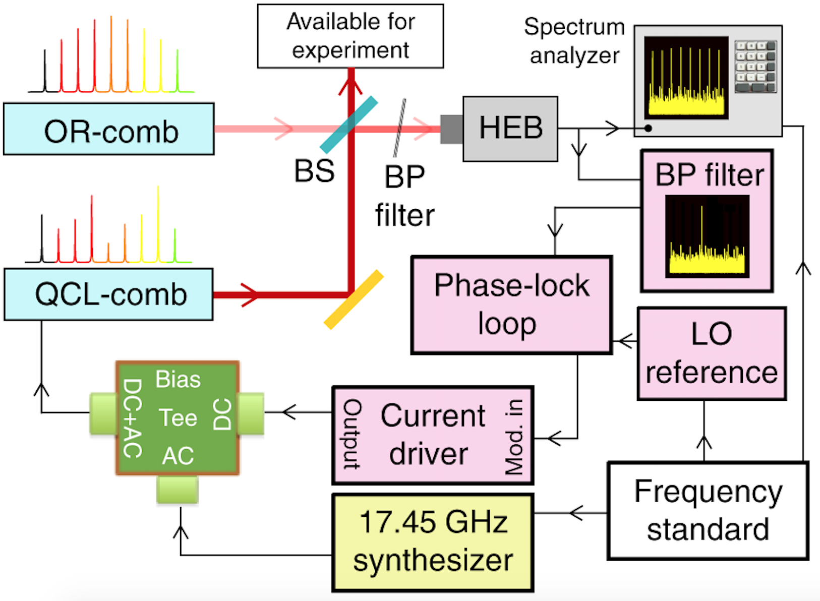
Miniaturized frequency comb sources across hard–to–access spectral regions, i.e. mid– and far–infrared, have long been sought. Four–wave–mixing based Quantum Cascade Laser combs (QCL–combs) are ideal candidates, in this respect, due to the unique possibility to tailor their spectral emission by proper nanoscale design of the quantum wells. We have demonstrated full–phase–stabilization of a QCL–comb against the primary frequency standard, proving independent and simultaneous control of the two comb degrees of freedom (modes spacing and frequency offset) at a metrological level. Each emitted mode exhibits a sub–Hz relative frequency stability, while a correlation analysis on the modal phases confirms the high degree of coherence in the device emission, over different power-cycles and over different days. The achievement of fully controlled, phase-stabilized QCL–comb emitters proves that this technology is mature for metrological-grade uses, as well as for an increasing number of scientific and technological applications.

Contact person: Luigi Consolino, INO Sesto Fiorentino

Nitrogen Soaking Promotes Lattice Recovery in Polycrystalline Hybrid Perovskites

A research team from two Institutes, IMM and NANOTEC, has found a very important innovative result in the field of photovoltaics applications by using hybrid Perovskites and Nitrogen.

Hybrid Perovskites are innovative materials that are sensitive to solar light with high conversion photon-electron performances.  Nitrogen is soaked into polycrystalline MAPbI3 via a post deposition mild thermal treatment under slightly overpressure conditions to promote its diffusion across the whole layer. A significant reduction of radiative recombination and a concurrent increase of light absorption, with a maximum benefit at 80 °C, are observed.

The achieved improvements are linked to a nitrogen‐assisted recovery of intrinsic lattice disorder at the grain shells along with a simultaneous stabilization of under-coordinated Pb2+ and MA+ cations through weak electrostatic interactions. Defect mitigation under N2 is reinforced in comparison to the benchmark behaviour under argon.

Such simple and low‐cost strategy can complement other stabilizing solutions for perovskite solar cells or light‐emitting diode engineering.

Contact persons: Alessandra Alberti - IMM Catania
Silvia Colella - NANOTEC Lecce

Phase contrast tomography at lab on chip scale by digital holography

High-throughput single-cell analysis is a challenging target for implementing advanced biomedical applications. An excellent candidate for this aim is label–free tomographic phase microscopy (TPM). We have reviewed some of the methods used to obtain TPM, analyzing advantages and disadvantages of each of them. Moreover, an alternative tomographic technique is described for live cells analysis, and future trends of the method are foreseen. In particular, by exploiting random rolling of cells while they are flowing along a microfluidic channel, it is possible to obtain phase-contrast tomography thus obtaining complete retrieval of both 3D–position and orientation of rotating cells. Thus, a priori knowledge of such information is no longer needed. This approach extremely simplifies the optical system avoiding any mechanical/optical scanning of light source. The proof is given for different classes of bio–samples, red–blood–cells (RBCs) and diatom algae. Accurate characterization of each type of cells is reported and compared to that obtained by other tomographic techniques.

Contact person: Francesco Merola,
ISASI Pozzuoli

Mechanisms and processes of pulsed laser ablation in liquids during nanoparticle production

In the last decade Pulsed Laser Ablation in Liquids (PLAL) has been widely investigated from the fundamental point of view, and various theories have been proposed. We have reconsidered previous works focused on specific processes and stages of the PLAL, in order to outline a modern and comprehensive point of view of the overall physical aspects of PLAL. With this aim, several simultaneous diagnostic methods have been applied during the production of metallic nanoparticles (NPs), i.e. optical emission spectroscopy and fast imaging for the investigation of the laser-induced plasma, shadowgraph for the study of the cavitation bubble, and Double Pulse Laser Ablation in Liquid (DP–LAL) and laser scattering for the investigation of NPs location and mechanisms of release in solution. The connection between the various stages of the DP–LAL allows understanding the main characteristics of the produced NPs and the typical timescales of the basic mechanisms involved in PLAL.

Contact person: Marcella Dell’Aglio, NANOTEC Bari

Ohmic contacts to gallium nitride materials

A comprehensive study of the mechanisms of Ohmic contact formation on GaN–based materials has been addressed. The optimal metallization schemes and processing conditions to obtain low resistance Ohmic contacts have been investigated, discussing the role of the single metals composing the stack and the modification induced by the thermal annealing, either on the metal layers or at the interface with GaN. Physical insights on the mechanism of Ohmic contact formation have been gained by correlating the temperature dependence of the electrical parameters with a morphological/structural analysis of the interface. In the case of the AlGaN/GaN systems, the influence of the heterostructure parameters on the Ohmic contacts has been taken into account adapting the classical thermionic field emission model to the presence of the two–dimensional electron gas. Finally, the “Au-free” metallization to AlGaN/GaN heterostructures has been deeply investigated, being this latter a relevant topic for the integration of GaN technology on large scale silicon devices fabrication.

Contact person: Giuseppe Greco, IMM Catania

Room–temperature superfluidity in a polariton condensate

Superfluidity – the suppression of scattering in a quantum fluid at velocities below a critical value – is one of the most striking manifestations of the collective behaviour typical of Bose–observed only at prohibitively low cryogenic temperatures. For atoms, this limit is imposed by the small thermal de Broglie wavelength, which is inversely related to the particle mass. Even in the case of ultralight quasiparticles such as exciton–polaritons, superfluidity has been demonstrated by the small binding energy of Wannier–Mott excitons, which sets the upper temperature limit. Here we demonstrate a transition from supersonic to superfluid flow in a polariton condensate under ambient conditions. This is achieved by using an organic microcavity supporting stable Frenkel exciton–polaritons at room temperature. This result paves the way not only for tabletop studies of quantum hydrodynamics, but also for room–temperature polariton devices that can be robustly protected from scattering.

Contact person: Daniele Sanvitto, NANOTEC Lecce

Spectral imaging and archival data in analysing Madonna of the rabbit paintings by Manet and Titian

A concise insight into the outputs provided by the latest prototype of visible–near infrared (Vis-NIR) multispectral scanner was presented. The analytical data acquired on an oil painting Madonna of the Rabbit by E. Manet were described. In this work, the Vis-NIR was complemented with X–ray fluorescence (XRF) mapping for the chemical and spatial characterization of several pigments. The spatially registered Vis–NIR data facilitated their processing by spectral correlation mapping (SCM) and artificial neural network (ANN) algorithm, respectively, for pigment mapping and improved visibility of pentimenti and of underdrawing style. The data provided several key elements for the comparison with a homonymous original work by Titian studied within the ARCHive LABoratory (ARCHLAB) transnational access project.

Contact person: Jana Striova, INO Florence

Dynamic scaling in natural swarms

Collective behavior in biological systems presents theoretical challenges beyond the borders of classical statistical physics. The lack of concepts such as scaling and renormalization is particularly problematic, as it forces us to negotiate details whose relevance is often hard to assess. In an attempt to improve this situation, we have presented experimental evidence of the emergence of dynamic scaling laws in natural swarms of midges. We found that spatio–temporal correlation functions in different swarms can be rescaled by using a single characteristic time, which grows with the correlation length with a dynamical critical exponent z ≈ 1, a value not found in any other standard statistical model. To check whether out–of–equilibrium effects may be responsible for this anomalous exponent, we run simulations of the simplest model of self–propelled particles and find z ≈ 2, suggesting that natural swarms belong to a novel dynamic universality class. This conclusion is strengthened by experimental evidence of the presence of non–dissipative modes in the relaxation, indicating that previously overlooked inertial effects are needed to describe swarm dynamics. The absence of a purely dissipative regime suggests that natural swarms undergo a near–critical censorship of hydrodynamics.

Contact person: Andrea Cavagna, ISC Rome

Control of doping level in semiconductors via self–limited grafting of phosphorus end terminated polymers

An effective bottom–up technology for precisely controlling the amount of dopant atoms tethered on silicon substrates has been presented. Polystyrene and poly (methyl methacrylate) polymers with narrow molecular weight distribution and end–terminated with a P–containing moiety were synthesized with different molar mass. The polymers were spin coated and subsequently end-grafted onto nondeglazed silicon substrates. P atoms were bonded to the surface during the grafting reaction, and their surface density was set by the polymer molar mass, according to the self-limiting nature of the “grafting to” reaction. Polymeric material was removed by O2 plasma hashing without affecting the tethered P–containing moieties on the surface. Repeated cycles of polymer grafting followed by plasma hashing led to a cumulative increase, at constant steps, in the dose of P atoms grafted to the silicon surface. P injection in the silicon substrate was promoted and precisely controlled by high–temperature thermal treatments. Sheet resistance measurements demonstrated effective doping of silicon substrate.

Contact person: Michele Perego, IMM Agrate Brianza

Landau–Zener transition in a continuously measured single–molecule spin transistor

We have monitored the Landau–Zener dynamics of a single–ion magnet inserted into a spin–transistor geometry. For increasing field–sweep rates, the spin reversal probability shows increasing deviations from that of a closed system. In the low–conductance limit, such deviations were shown to result from a dephasing process. In particular, the observed behaviors were successfully simulated by means of an adiabatic master equation, with time averaged dephasing (Lindblad) operators. The time average was tentatively interpreted in terms of the finite time resolution of the continuous measurement.

Contact person: Filippo Troiani, NANO Modena

Femtosecond laser micromachining: a powerful tool for integrated diamond quantum photonics

Diamond’s nitrogen vacancy (NV) center is an optically active defect with long spin coherence times, showing great potential for both efficient nanoscale magnetometry and quantum information processing schemes with room temperature operations. In an international collaborative endeavour led by CNR-IFN Milano, femtosecond laser writing has been shown as a powerful tool for both the formation of buried 3D optical components and single NVs in the bulk of diamond. Recently, an integrated device consisting of laser-written photonic waveguides in ultrapure diamond aligned to sub-micron resolution to single laser-written NVs have been realized. Laser written optical waveguides have been used to excite and collect photoluminescence signal from single NVs. The results obtained paves the way towards complex integrated diamond quantum devices with optically connected single photons from NVs for spin-based magnetic, electric and thermal sensing.

Contact person: Shane Eaton, IFN Milano

Kinetic Inductance Detector (KID) Arrays for the OLIMPO programme

Kinetic Inductance Detectors (KIDs) are a novel type of superconducting photon detectors firstly developed in 2003 and currently employed in several research fields. In particular, they got a rapid employment in astrophysics as high-sensitivity detectors for frequencies ranging from the far-infrared to X-rays.  In the framework of the OLIMPO mission, an Italian programme in collaboration with Sapienza University in Rome, we developed  four KID arrays simultaneously investigating four different bands of the microwave spectrum (centred at 150 GHz, 200 GHz, 350 GHz, and 480 GHz). They  will be mounted on the OLIMPO telescope with the aim of  measuring the anisotropy of cosmic microwave background radiation and cluster of galaxies and early galaxies with unparalleled precision. The OLIMPO’s KID arrays have been realized by electron beam lithography, thin film deposition and lift-off processes. They consist of 23 to 43 KIDs patterned in a 25-nm thick aluminium film on high resistivity Si wafers connected capacitively to a same coplanar feedline for their simultaneous reading. OLIMPO will be the first telescope equipped with KIDs and mounted on a long-term stratospheric balloon to fly. The mission will be launched by ASI in June 2018.

Contact person: Giorgio Pettinari, IFN - CNR Roma

Topological order and thermal equilibrium in polariton condensates

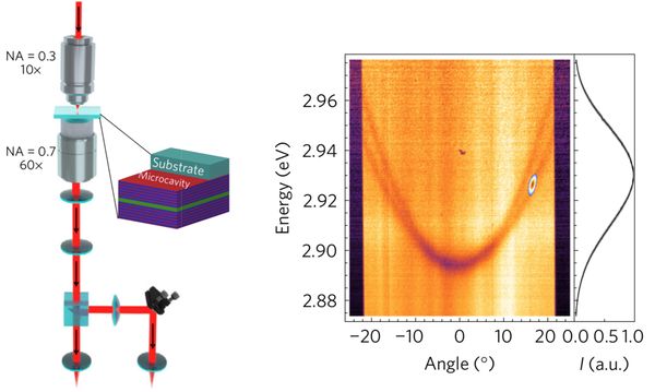
The Berezinskii–Kosterlitz–Thouless phase transition from a disordered to a quasi-ordered state, mediated by the proliferation of topological defects in two dimensions, governs seemingly remote physical systems ranging from liquid helium, ultracold atoms and superconducting thin films to ensembles of spins. We have observed such a transition in a short–lived gas of exciton–polaritons, bosonic light–matter particles in semiconductor microcavities. The observed quasi–ordered phase, characteristic for an equilibrium two–dimensional bosonic gas, with a decay of coherence in both spatial and temporal domains with the same algebraic exponent, is reproduced with numerical solutions of stochastic dynamics, proving that the mechanism of pairing of the topological defects (vortices) is responsible for the transition to the algebraic order. This is made possible thanks to long polariton lifetimes in high–quality samples and in a reservoir–free region. Our results show that the joint measurement of coherence both in space and time is required to characterize driven–dissipative phase transitions and enable the investigation of topological ordering in open systems.

Contact person: Dario Ballarini, NANOTEC Lecce

Carbon nanotubes as excitonic insulators

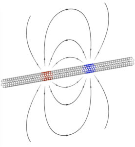
Fifty years ago Walter Kohn speculated that a zero-gap semiconductor might be unstable against the spontaneous generation of excitons–electron–hole pairs bound together by Coulomb attraction. The reconstructed ground state would then open a gap breaking the symmetry of the underlying lattice, a genuine consequence of electronic correlations. We have shown that this excitonic insulator is realized in zero–gap carbon nanotubes by performing first–principles calculations through many–body perturbation theory as well as quantum Monte Carlo. The excitonic order modulates the charge between the two carbon sublattices opening an experimentally observable gap, which scales as the inverse of the tube radius and weakly depends on the axial magnetic field. Our findings call into question the Luttinger liquid paradigm for nanotubes and provide tests to experimentally discriminate between excitonic and Mott insulators.

Contact person: Daniele Varsano, NANO Modena

Rational design of molecular hole–transporting materials for perovskite solar cells: direct versus inverted device configurations

Due to a still limited understanding of the reasons making 2,2/,7,7/–tetrakis(N,N–di–p–methoxyphenylamine)–9,9/–spirobifluorene (Spiro–OMeTAD) the state–of–the–art hole–transporting material (HTM) for emerging photovoltaic applications, the molecular tailoring of organic components for perovskite solar cells (PSCs) lacks in solid design criteria. Charge delocalization in radical cationic states can undoubtedly be considered as one of the essential prerequisites for an HTM, but this aspect has been investigated to a relatively minor extent. In marked contrast with the 3–D structure of Spiro–OMeTAD, truxene–based HTMs Trux1 and Trux2 have been employed for the first time in PSCs fabricated with a direct (nip) or inverted (pin) architecture, exhibiting a peculiar behavior with respect to the referential HTM. Notwithstanding the efficient hole extraction from the perovskite layer exhibited by Trux1 and Trux2 in direct configuration devices, their photovoltaic performances were detrimentally affected by their poor hole transport. Conversely, an outstanding improvement of the photovoltaic performances in dopant–free inverted configuration devices compared to Spiro–OMeTAD was recorded, ascribable to the use of thinner HTM layers. The rationalization of the photovoltaic performances exhibited by different configuration devices discussed in this paper can provide new and unexpected prospects for engineering the interface between the active layer of perovskite–based solar cells and the hole transporters.

Contact person: Luisa De Marco, NANOTEC Lecce

Electrostatic mechanophores in tuneable light–emitting piezopolymer nanowires

Electromechanical coupling through piezoelectric polymer chains allows the emission of organic molecules in active nanowires to be tuned. This effect is evidenced by highly bendable arrays of counter–ion dye–doped nanowires made of a poly(vinylidenefluoride) copolymer. A reversible redshift of the dye emission is found upon the application of dynamic stress during highly accurate bending experiments. By density functional theory calculations it is found that these photophysical properties are associated with mechanical stresses applied to electrostatically interacting molecular systems, namely to counter–ion–mediated states that involve light–emitting molecules as well as charged regions of piezoelectric polymer chains. These systems are an electrostatic class of supramolecular functional stress–sensitive units, which might impart new functionalities in hybrid molecular nanosystems and anisotropic nanostructures for sensing devices and soft robotics.

Contact person: Luana Persano, NANO Pisa

Detection of food and skin pathogen microbiota by means of an electronic nose based on metal oxide chemiresistors

We have analyzed the potentiality of a mixed array merging the nanowire and thin film metal oxide technologies to develop an electronic nose as a tool to monitor the human skin and food pathogen microbiota. Nanowire and thin film sensors have been fabricated, characterized and then integrated together to develop a hybrid device that can enhance the sensing performance. Different blends of microorganisms grown in artificial sweat have been tested. Classical techniques, like gas chromatography–mass spectrometry (GC–MS) with solid phase micro extraction (SPME) have been employed in parallel, in order to have a multidisciplinary approach and a consistent data set. The obtained results demonstrate the potentiality of the proposed electronic nose to discriminate between the different blends of microorganisms and to follow up microbiota growth inside the blends.

Contact person: Estefanìa Nùñez Carmona, INO Brescia

0–π phase–controllable thermal Josephson junction

We have reported the first experimental realization of a thermal Josephson junction whose phase bias can be controlled from 0 to π. This is obtained thanks to a superconducting quantum interferometer that allows full control of the direction of the coherent energy transfer through the junction. This possibility, in conjunction with the completely superconducting nature of our system, provides temperature modulations with an unprecedented amplitude of about 100 mK and transfer coefficients exceeding 1 K per flux quantum at 25 mK. Then, this quantum structure represents a fundamental step towards the realization of caloritronic logic components such as thermal transistors, switches and memory devices. These elements, combined with heat interferometers and diodes, would complete the thermal conversion of the most important phase–coherent electronic devices and benefit cryogenic microcircuits requiring energy management, such as quantum computing architectures and radiation sensors.

Contact person: Antonio Fornieri, NANO Pisa

Electronic states of silicene allotropes on Ag(111)

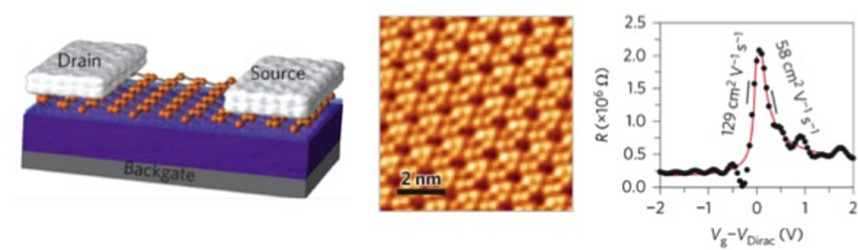
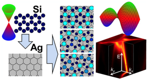
We have compared the electronic structure of (4×4), (√13×√13) R 13.9° and (2√3×2√3) R 30° silicene monolayers on Ag(111) by means of angle–resolved photoemission spectroscopy and first–principles calculations. We have found that all phases display similar Ag–derived interface states and s bands weakly perturbed by the substrate interaction. Intense spectral features, including those previously attributed to s band emission from the (2√3×2√3) R 30° structure, are found to originate from umklapp replicas of the Ag interface state and Ag sp–bulk bands. All the examined silicene allotropes do not display the characteristic Dirac cones of free–standing silicene, proving that the p bands are strongly modified by the interaction with the substrate bands independently of the structural detail of the allotrope.

Contact person: Polina Sheverdyaeva, ISM Trieste

Holographic imaging reveals the mechanism of wall entrapment in swimming bacteria

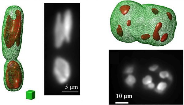
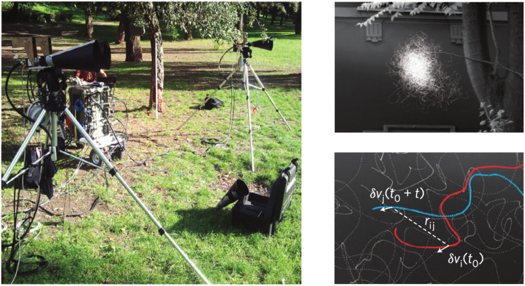
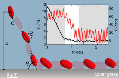
Self–propelled particles, both biological and synthetic, are stably trapped by walls and develop high concentration peaks over bounding surfaces. In swimming bacteria, like E. coli, the physical mechanism behind wall entrapment is an intricate mixture of hydrodynamic and steric interactions with a strongly anisotropic character. We have demonstrated that, by using a combination of three-axis holographic microscopy and optical tweezers, it is possible to obtain volumetric reconstructions of individual E. coli cells that are sequentially released at a controlled distance and angle from a flat solid wall. We have found that hydrodynamic couplings can slow down the cell before collision, but reorientation only occurs while the cell is in constant contact with the wall. In the trapped state, all cells swim with the average body axis pointing into the surface. The amplitude of this pitch angle is anticorrelated to the amplitude of wobbling, thus indicating that entrapment is dominated by near–field couplings between the cell body and the wall.


Contact person: Silvio Bianchi, NANOTEC Rome

Interface electrical properties of Al2O3 thin films on graphene obtained by atomic layer deposition with an in situ seedlike layer

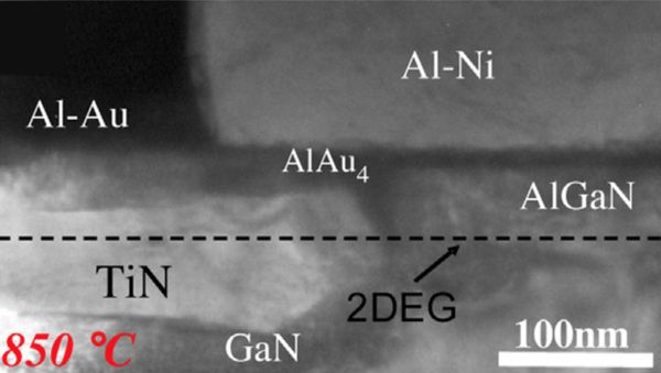
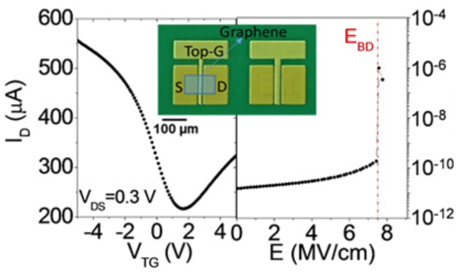
High–quality thin insulating films on graphene (Gr) are essential for field-effect transistors (FETs) and other electronics applications of this material. We have reported a detailed morphological, structural, and electrical investigation of Al2O3 thin films grown by a two–steps ALD process on a large area Gr membrane residing on an Al2O3–Si substrate. This process consists of the H2O–activated deposition of a Al2O3 seed layer a few nanometers in thickness, performed in situ at      100 °C, followed by ALD thermal growth of Al2O3 at 250 °C. Nanoscale–resolution mapping of the current through the dielectric by conductive atomic force microscopy (CAFM) demonstrated an excellent laterally uniformity of the film. Analysis of the transfer characteristics of Gr field–effect transistors (GFETs) allowed us to evaluate the relative dielectric permittivity (ε = 7.45) and the breakdown electric field (EBD = 7.4 MV/cm) of the Al2O3 film as well as the transconductance and the holes field-effect mobility (about 1200 cm2 V–1 s–1).

Contact person: Gabriele Fisichella, IMM Catania

Synthetic dimensions with magnetic fields and local interactions in photonic lattices

We have investigated how one can realize a photonic device that combines synthetic dimensions and synthetic magnetic fields with spatially local interactions. Using an array of ring cavities, the angular coordinate around each cavity spans the synthetic dimension. The synthetic magnetic field arises from the circumstance that intercavity photon hopping is associated with a change of angular momentum. Photon-photon interactions are local in the periodic angular coordinate around each cavity. We have also pointed out experimentally observable consequences of the synthetic magnetic field and of the local interactions.

Contact person: Iacopo Carusotto, INO Trento

Bipolar patterning of polymer membranes by pyroelectrification

We have reported a voltage–free pyroelectrification (PE) process able to induce permanent and 2D patterned dipoles into polymer films, thus producing freestanding bipolar membranes. A single thermal stimulus triggers simultaneously the glass transition and the dipole orientation in the polymer. The technique is surprisingly easy to accomplish since the polymer solution is simply spin–coated onto a pyroelectric lithium niobate crystal that, during the thermal stimulus, generates spontaneously a surface charge density strong enough to orient the polymer dipoles.

Contact person: Simonetta Grilli, ISASI Pozzuoli


Tunable Esaki effect in catalyst–free InAs/GaSb core–shell nanowires

We have demonstrated tunable bistability and a strong negative differential resistance in InAs/GaSb core–shell nanowire devices embedding a radial broken–gap heterojunction. Nanostructures have been grown using a catalyst-free synthesis on a Si substrate. Current–voltage characteristics display a top peak–to–valley ratio of 4.8 at 4.2 K and 2.2 at room temperature. The Esaki effect can be modulated – or even completely quenched – by field effect, by controlling the band bending profile along the azimuthal angle of the radial heterostructure. Hysteretic behavior is also observed in the presence of a suitable resistive load. Our results indicate that high–quality broken–gap devices can be obtained using Au–free growth.

Contact person: Mirko Rocci, NANO Pisa

Toward cavity quantum electrodynamics with hybrid photon gap–plasmon states

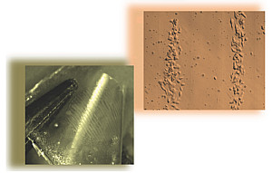
Combining localized surface plasmons (LSPs) and diffractive surface waves (DSWs) in metallic nanoparticle gratings leads to the emergence of collective hybrid plasmonic–photonic modes known as surface lattice resonances (SLRs). These show reduced losses and therefore a higher Q factor with respect to pure LSPs, at the price of larger volumes V. By using aluminum nanoparticle square gratings with unit cells consisting of narrow–gap disk dimers (a geometry featuring a very small modal volume) we have demonstrated that an enhancement of the Q/V ratio with respect to the pure LSP and DSW is obtained for SLRs with a well–defined degree of plasmon hybridization. Simultaneously, we have reported a 5 times increase of the Q/V ratio for the gap–coupled LSP with respect to that of the single nanoparticle. The results of this work open the way toward more efficient applications for the exploitation of excitonic nonlinearities in hybrid plasmonic platforms.

Contact person: Milena De Giorgi, NANOTEC Lecce

Ambipolar MoS2 transistors by nanoscale tailoring of Schottky barrier using oxygen plasma functionalization

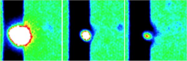
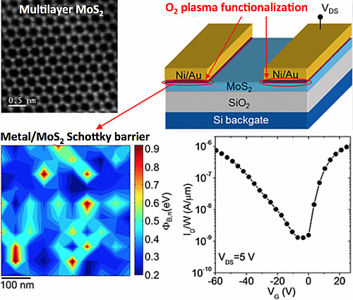
Hole transport in MoS2 field–effect transistors (FETs) is typically hampered by the high Schottky barrier height (SBH) for holes at source/drain contacts, due to the Fermi level pinning close to the conduction band. We have shown that the SBH of multilayer MoS2 surface can be tailored at nanoscale using soft O2 plasma treatments. Nanoscale current–voltage mapping by Conductive Atomic Force Microscopy showed that the SBH maps can be conveniently tuned starting from a narrow SBH distribution (from 0.2 to 0.3 eV) in the case of pristine MoS2 to a broader distribution (from 0.2 to 0.8 eV) after 600 s O2 plasma treatment, which allows both electron and hole injection. Back-gated multilayer MoS2 FETs, fabricated by self–aligned deposition of source/drain contacts in the O2 plasma functionalized areas, exhibit ambipolar current transport with on/off current ratio Ion/Ioff ≈ 103 and field–effect mobilities of 11.5 and 7.2 cm2 V–1s–1 for electrons and holes, respectively.

Contact person: Filippo Giannazzo, IMM Catania

Anisotropic MoS2 nanosheets grown on self–organized nanopatterned substrates

We have presented a novel approach to introduce a one–directional anisotropy in MoS2 nanosheets via chemical vapor deposition (CVD) onto rippled patterns prepared on ion–sputtered SiO2/Si substrates. The optoelectronic properties of MoS2 are dramatically affected by the rippled MoS2 morphology both at the macro– and the nanoscale. In particular, strongly anisotropic phonon modes are observed depending on the polarization orientation with respect to the ripple axis. Moreover, the rippled morphology induces localization of strain and charge doping at the nanoscale, thus causing substantial redshifts of the phonon mode frequencies and a topography–dependent modulation of the MoS2 work–function, respectively. This study paves the way to a controllable tuning of the anisotropy via substrate pattern engineering in CVD–grown 2D nanosheets.

Contact person: Christian Martella, IMM–CNR Agrate Brianza

Complex active optical networks as a new laser concept

We have investigated complex optical networks containing one or more gain sections, and we have reported the evidence of lasing action; the emission spectrum reflects the topological disorder induced by the connections. A theoretical description compares well with the measurements, mapping the networks to directed graphs and showing the analogies with the problem of quantum chaos on graphs. We have shown that the interplay of chaotic diffusion and amplification leads to an emission statistic with characteristic heavy tails: for different topologies, we have provided an unprecedented experimental demonstration of Lévy statistics, expected for random lasers, for a continuous–wave pumped system.

Contact person: Stefano Lepri, ISC-CNR Sesto Fiorentino

Repulsive Fermi polarons in a resonant mixture of ultracold 6Li atoms

We employ radio–frequency spectroscopy to investigate a polarized spin mixture of ultracold 6Li atoms close to a broad Feshbach scattering resonance. Focusing on the regime of strong repulsive interactions, we observe well-defined coherent quasiparticles even for unitarity–limited interactions. We characterize the many-body system by extracting the key properties of repulsive Fermi polarons: the energy E+, the effective mass m*, the residue Z, and the decay rate Γ. Above a critical interaction, E+ is found to exceed the Fermi energy of the bath, while m* diverges and even turns negative, thereby indicating that the repulsive Fermi liquid state becomes energetically and thermodynamically unstable.

Contact person: Francesco Scazza, INO-CNR Sesto Fiorentino

Organic gelators as growth control agents for stable and reproducible hybrid perovskite–based solar cells

We have used the concept based on low molecular–weight organic gelators to hybrid halide perovskite–based materials. Our measurements reveal that organic gelators beneficially influence the nucleation and growth of the perovskite precursor phase. This can be exploited for the performance that not only is enhanced by about 25% compared to solar cells where the active layer was produced without the use of a gelator but that also feature a higher stability to moisture and a reduced hysteresis. The proposed approach provides a general method to render the film–formation of hybrid perovskites more reliable and robust.

Contact person: Silvia Colella, NANOTEC-CNR Lecce

Atomistic origins of CH3NH3PbI3 degradation to PbI2 in vacuum

We have studied the mechanisms of CH3NH3PbI3 degradation and its transformation to PbI2 by means of X–ray diffraction and the density functional theory. The experimental analysis has shown that the material can degrade in both air and vacuum conditions, with humidity and temperature–annealing strongly accelerating such process. Based on ab–initio calculations, we have argued that even in the absence of humidity, a decomposition of the perovskite structure can take place through the statistical formation of molecular defects with a non–ionic character, whose volatility at surfaces should break the thermodynamic defect equilibrium.

Contact person: Ioannis Deretzis, IMM–CNR Catania

Methylammonium rotational dynamics in lead halide perovskite by classical molecular dynamics: the role of temperature

An interatomic model potential for molecular dynamics was derived from first–principles and used to study the molecular rotations and relaxation times in methylammonium lead halide, considered the prototypical example of a hybrid crystal with a strong reorientational dynamics. Within the limits of a simple ionic scheme, the potential is able to catch the main qualitative features of the material at zero and finite temperature and opens the way to the development of classical potentials for hybrid perovskites. This work has clarified the temperature dependence of the relaxation times and the interpretation of the experimental data in terms of the different mechanisms contributing to the molecule dynamics.

Contact person: Alessandro Mattoni, IOM–CNR Cagliari

Tunable spin polarization and superconductivity in engineered oxide interfaces

We have shown that a fully electric–field–tunable spin–polarized and superconducting quasi–2D electron system (q2DES) can be artificially created by inserting a few unit cells of delta doping EuTiO3 at the interface between LaAlO3 and SrTiO3 oxides. Spin polarization emerges below the ferromagnetic transition temperature of the EuTiO3 layer (TFM = 6–8 K) and is due to the exchange interaction between the magnetic moments of Eu–4f and of Ti–3d electrons. Moreover, in a large region of the phase diagram, superconductivity sets in from a ferromagnetic normal state. The occurrence of magnetic interactions, superconductivity and spin–orbit coupling in the same q2DES makes the LaAlO3/EuTiO3/SrTiO3 system an intriguing platform for the emergence of novel quantum phases in low–dimensional materials.

Contact person: Marco Salluzzo, SPIN–CNR Napoli

Local equilibrium in bird flocks

We have introduced a novel dynamical inference technique, based on the principle of maximum entropy, which accommodates network rearrangements and overcomes the problem of slow experimental sampling rates. We have used this method to infer the strength and range of alignment forces from data of starling flocks. We have found that local bird alignment occurs on a much faster timescale than neighbour rearrangement. Accordingly, equilibrium inference, which assumes a fixed interaction network, gives results consistent with dynamical inference. We conclude that bird orientations are in a state of local quasi–equilibrium over the interaction length scale, providing firm ground for the applicability of statistical physics in certain active systems.

Contact person: Massimiliano Viale, ISC–CNR Univ. Roma La Sapienza

Red blood cell as an adaptive optofluidic microlens

We have shown that a suspended red blood cell (RBC) behaves as an adaptive liquid–lens at microscale, thus demonstrating its imaging capability and tunable focal length. In fact, thanks to the intrinsic elastic properties, the RBC can swell up from disk volume of 90 fl up to a sphere reaching 150 fl, varying focal length from negative to positive values. These live optofluidic lenses can be fully controlled by triggering the liquid buffer’s chemistry. Real–time accurate measurement of tunable focus capability of RBCs is reported through dynamic wavefront characterization, showing agreement with numerical modelling. Moreover, in analogy to adaptive optics testing, blood diagnosis is demonstrated by screening abnormal cells through focal–spot analysis applied to an RBC ensemble as a microlens array.

Contact person: Lisa Miccio, ISASI–CNR Pozzuoli

Electrospun amplified fiber optics

We have reported on near–infrared polymer fiber amplifiers working over a band of about 20 nm. The fibers are cheap, spun with a process entirely carried out at room temperature, and shown to have amplified spontaneous emission with good gain coefficients and low levels of optical losses (a few cm–1). The amplification process is favored by high fiber quality and low self–absorption. The found performance metrics appear to be suitable for short–distance operations, and the large variety of commercially available doping dyes might allow for effective multi–wavelength operations by electrospun amplified fiber optics.

Contact person: Dario Pisignano, NANO–CNR Pisa

Resistive switching in high–density nanodevices fabricated by block copolymer self–assembly

By exploiting a bottom-up fabrication approach based on block copolymer self-assembling, we obtained the parallel production of bilayer Pt/Ti top electrodes arranged in periodic arrays over the HFO2/TiN surface, building memory devices with a diameter of 28 nm and a density of 5´1010 devices/cm2. For an electrical characterization, the sharp conducting tip of an atomic force microscope was adopted for a selective addressing of the nanodevices. The presence of devices showing high conductance in the initial state was directly connected with scattered leakage current paths in the bare oxide film, while with bipolar voltage operations we obtained reversible set/reset transitions irrespective of the conductance variability in the initial state.

Contact person: Michele Perego, IMM–CNR Agrate Brianza

Micromotors with asymmetric shape that efficiently convert light into work by thermocapillary effects

The direct conversion of light into work allows the driving of micron-sized motors in a contactless, controllable and continuous way. We have shown that microfabricated gears, sitting on a liquid–air interface, can efficiently convert absorbed light into rotational motion through a thermocapillary effect. We have demonstrated rotation rates up to 300 r.p.m. under wide–field illumination with incoherent light. Our analysis shows that thermocapillary propulsion is one of the strongest mechanisms for light actuation at the micron– and nanoscale.

Contact person: Claudio Maggi, NANOTEC–CNR Roma

Silicene field-effect transistors operating at room temperature

We have reported a silicene field–effect transistor, corroborating theoretical expectations regarding its ambipolar Dirac charge transport, with a measured room–temperature mobility of about 100 cm2 V–1 s–1 attributed to acoustic phonon–limited transport and grain boundary scattering. These results are enabled by a growth–transfer–fabrication process that we have devised silicene encapsulated delamination with native electrodes. This approach addresses a major challenge for material preservation of silicene during transfer and device fabrication and is applicable to other air–sensitive two–dimensional materials such as germanene and phosphorene. Silicene’s allotropic affinity with bulk silicon and its low-temperature synthesis compared with graphene or alternative two–dimensional semiconductors suggest a more direct integration with ubiquitous semiconductor technology.

Contact person: Alessandro Molle, IMM–CNR Agrate Brianza

Triple–helical nanowires by tomographic rotatory growth for chiral photonics

We have reported three dimensional triple–helical nanowires, engineered by the innovative tomographic rotatory growth, on the basis of focused ion beam-induced deposition. These three dimensional nanostructures show up to 37% of circular dichroism in a broad range (500–1,000 nm), with a high signal-to-noise ratio (up to 24 dB). Optical activity of up to 8° only due to the circular birefringence is also shown, tracing the way towards chiral photonic devices that can be integrated in optical nanocircuits to modulate the visible light polarization.

Contact person: Vittorianna Tasco, NANOTEC–CNR Lecce

Nanoscale phase engineering of thermal transport with a Josephson heat modulator

We have realized the first balanced Josephson heat modulator designed to offer full control at the nanoscale over the phase-coherent component of thermal currents. Our device provides magnetic–flux–dependent temperature modulations up to 40 mK in amplitude with a maximum of the flux–to–temperature transfer coefficient reaching 200 mK per flux quantum at a bath temperature of 25 mK. Foremost, it demonstrates the exact correspondence in the phase engineering of charge and heat currents, breaking ground for advanced caloritronic nanodevices such as thermal splitters, heat pumps and time–dependent electronic engines.

Contact person: Francesco Giazotto, NANO–CNR Pisa

Josephson effect in fermionic superfluids across the BEC–BCS crossover

We have reported on the observation of the Josephson effect between two fermionic superfluids coupled through a thin tunneling barrier. We have shown that the relative population and phase are canonically conjugate dynamical variables throughout the crossover from the molecular Bose-Einstein condensate (BEC) to the Bardeen–Cooper–Schrieffer (BCS) superfluid regime. For larger initial excitations from equilibrium, the dynamics of the superfluids become dissipative, which we ascribe to the propagation of vortices through the superfluid bulk. Our results highlight the robust nature of resonant superfluids.

Contact person: Giacomo Roati, INO–CNR Sesto Fiorentino